


Make: ULVAC PHI
Model: VersaProbe III
Mode: XPS & UPS
XPS is a surface-sensitive quantitative spectroscopic technique that can identify the elemental composition within a material (till 1 µm) or on its surface, with their chemical state, and overall electronic structure and density of the electronic states in the material. XPS is used to characterize the surfaces of diverse materials such as inorganic compounds (minerals), semiconductors, organic compounds, and thin films and coatings on natural and engineered materials.
Make : FEI
Model: QUANTA 200F
Mode : SE, BSE, & EDX
Specifications
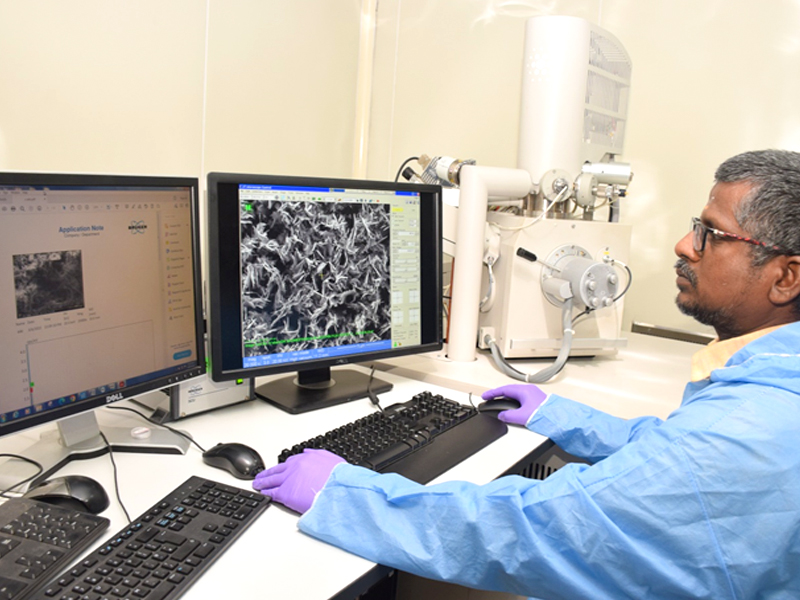
Field emission scanning electron microscopy (FESEM) provides topographical and elemental information at magnifications of 10x to 300,000x with virtually unlimited depth of field. Compared with convention scanning electron microscopy (SEM), field emission SEM (FESEM) produces clearer, less electrostatically distorted images with spatial resolution down to 1.5 nm that is three to six times better
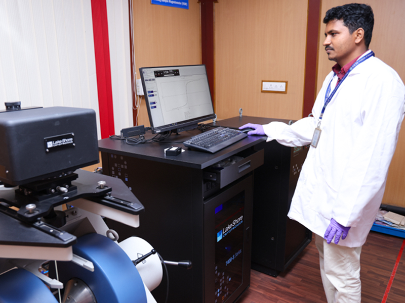
Make: Lake Shore Cryotronics
Model: 7407-S
Mode: High Temperature
(300K- 1000K)
Low Temperature
(300K – 15K) Room Temperature Operation
VSM is used to measure the magnetic behaviour of magnetic materials. It is a scientific instrument that measures magnetic properties based on Faraday’s Law of Induction, which tells us that a changing magnetic field will produce an electric field. This electric field can be measured and can tell us information about the changing magnetic field.
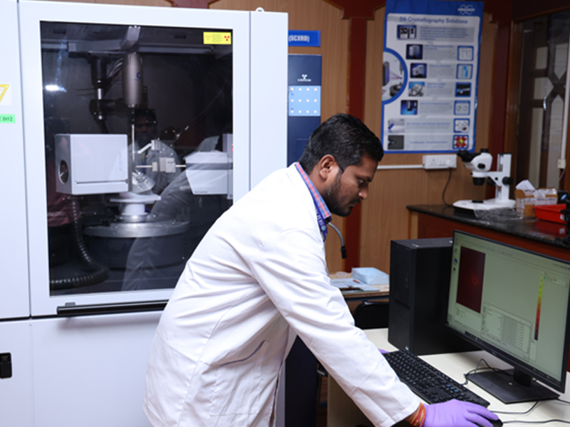
Make: Bruker
Model: D8 QUEST
Mode: Single Crystals
Single crystal X-ray diffraction (XRD) is a powerful technique used to determine the atomic and molecular structure of crystalline materials. It provides detailed information about the arrangement of atoms within a crystal lattice, revealing the positions of atoms and the distance between them.
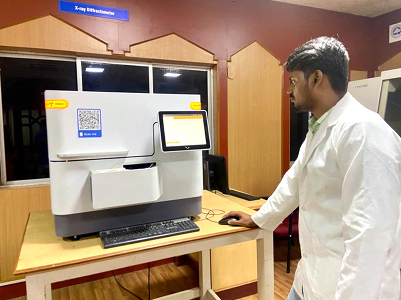
Make: PANalytical
Model: Benchtop
Mode: Powder & Thin Film
Specification
An X-Ray Diffraction Spectrometer (XRD) instrument is a device used to perform X-ray diffraction analysis on various materials. It is a powerful tool for studying the crystallographic properties of solids, liquids, and powders. XRD instruments can provide valuable information about atomic arrangement within a material’s lattice, crystal structure, phase composition, crystal orientation, and other structural characteristics.
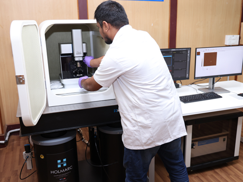
Make: Park System Corporation
Model: NX 10
Mode: AFM, EFM, PFM& KPFM
Atomic Force Microscopy (AFM) is a nanoscale imaging technique using a sharp tip on a cantilever to scan surfaces. It provides high-resolution topographical maps of materials, revealing atomic and molecular structures. AFM is a non-destructive and versatile method. The versatility of AFM allows researchers to study various materials, such as semiconductor films, polymers and biological samples. It offers real-time imaging and quantitative data on forces and interactions, making it crucial in nanotechnology and materials science.
Make: LINSEIS
Model: LZT meter
Mode: LSR/LFA
The LZT-Meter offers an all-in-one solution for the independent determination of thermal conductivity using the flash method and measurements of electrical resistance and Seebeck coefficient (known from the LSR platform).
Make : SHIMADZU UV 5600 PLUS
Features
Wide wavelength range:185-3300 nm
Absolute specular reflectance
Liquid samples testing setup
Low noise: 0.00003 Abs at 1500 nm
UV-Visible spectroscopy is a widely used simple and non-destructive technique, that investigates the absorption of ultraviolet (UV) and visible light by molecules. It provides valuable information about the electronic structure and the presence of certain functional groups in organic and inorganic compounds. The principle behind UV-Visible spectroscopy is based on the interaction of light with matter. When a sample is exposed to UV or visible light, some of the photons are absorbed by the molecules within the sample, causing transitions in their electron energy levels. These transitions are associated with the excitation of electrons from lower energy levels to higher energy levels. The energy difference between these levels corresponds to specific wavelengths of light.
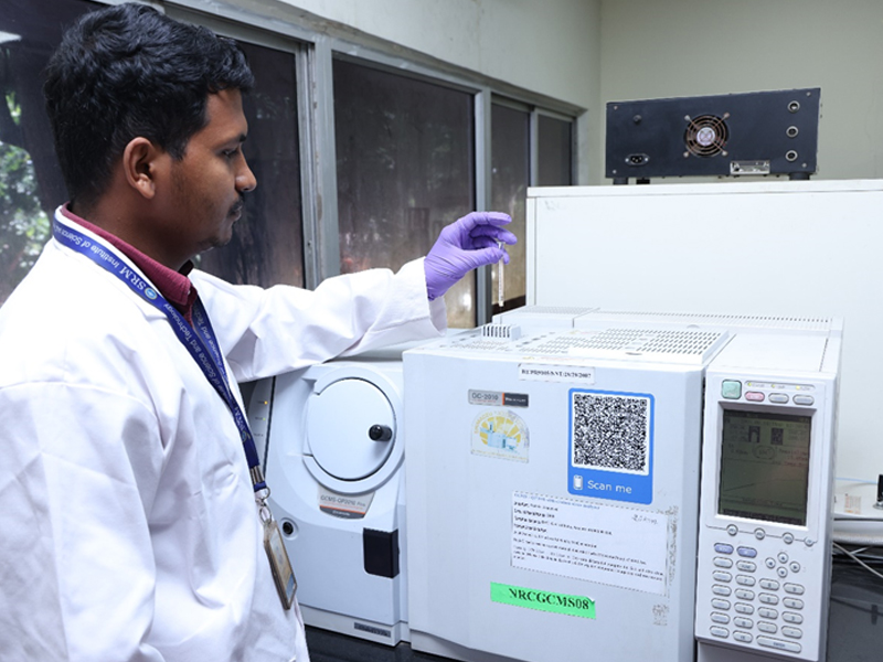
Make: Toshvin Analytical
Features
Temperature range : 4 – 450 ℃
Carrier gas control : Advanced flow controller
Detectors : FID, BID, TCD, ECD, MS
GCMS is a powerful analytical technique that combines gas chromatography and mass spectrometry to identify and quantify different substances within a sample. GCMS instruments have a wide range of applications in various fields due to their high sensitivity, selectivity, and ability to analyze complex mixtures.
Make: SHIMADZU IRTRACER 100
Features
Wavenumber range : 7800-350 cm-1
Sensitivity : S/N ratio of 60000:1
High speed : 20 spectra/ second
A Fourier Transform InfraRed (FT-IR) Spectrometer is an instrument which acquires broadband Near InfraRed (NIR) to Far InfraRed (FIR) spectra. It is a technique used to obtain an infrared spectrum of absorption or emission of a solid, liquid, or gas. An FTIR spectrometer simultaneously collects high-resolution spectral data over a wide spectral
Manufacturer: SCIENCETECH, PTS-2-QE
Features
IV testing, Spectral response, QE
Bias Light Source: AAA (ASTM E927) Solar Simulator
Quantum Efficiency measurement system with spectra range of 250-2500 nm. Monochromatic light source power up to 150 W Xe arc lamp. It can measure large capacitance of solar cells with DC/AC mode measurement capability
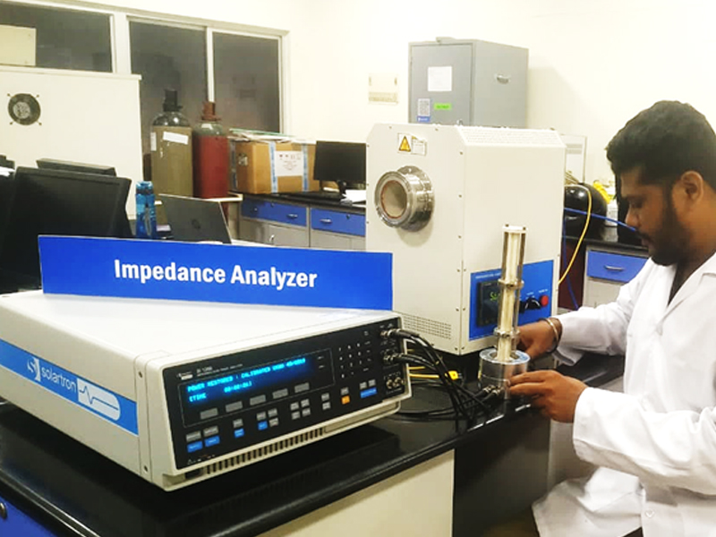
Make: AMETEK SOLARTRON 1260A
Features
Frequency range : 10 µHz to 32 MHz
Temperature range : RT – 800 ℃
DC bias voltage : ± 40 V
AC voltage max : 3 V
Impedance analysers are a class of instruments which measure complex electrical impedance as a function of frequency. This involves the phase sensitive measurement of current and voltage applied to a device under test while the measurement frequency is varied over the course of the measurement. Impedance is an important parameter used to characterize electronic components, electronic circuits, and the materials used to make components. Impedance analysis can also be used to characterize materials exhibiting dielectric behavior such as biological tissue, foodstuffs or geological samples.
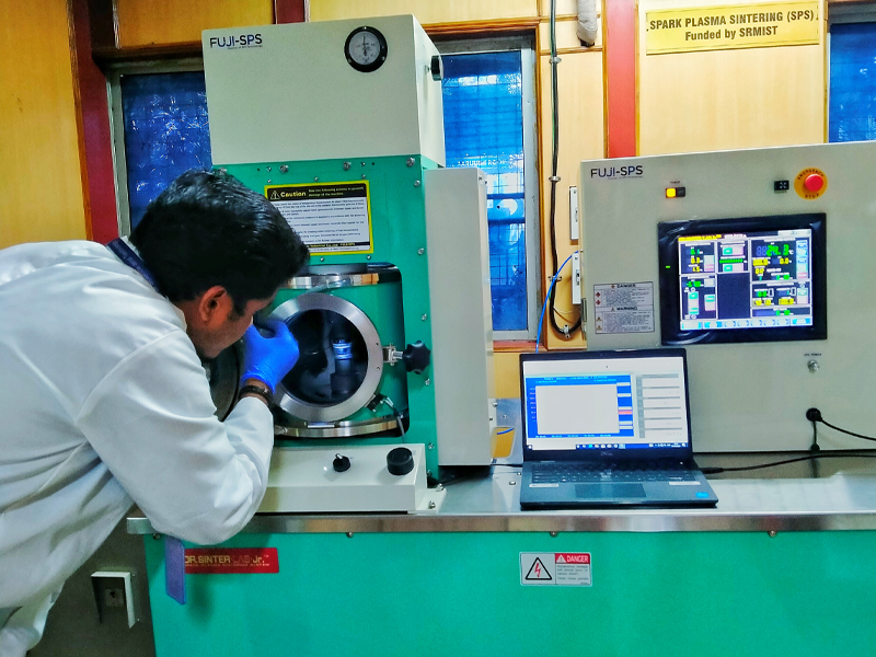
Supplier: FUJI Electronics Industrial Co., Ltd.
Model: FUJI SPS
Operation: Plasma sintering
Spark Plasma Sintering (SPS) is an innovative synthesis process that has garnered significant attention in advanced material development. This technique utilizes ON-OFF pulse DC voltage/current to fabricate previously challenging materials to create effectively. Here, this instrument can reach above 1000 °C within a few minutes and pressing pressure of about 50 MPa. SPS offers a promising solution to produce new materials that were once difficult to synthesize using conventional methods.
Supplier: VT Vacuum, Bangalore
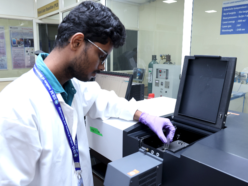
Dep. Chamber: Kurt J.Leskar , USA
Vacuum Sys: Agilent Technologies, USA
LASER: Excimer lasers, Germany
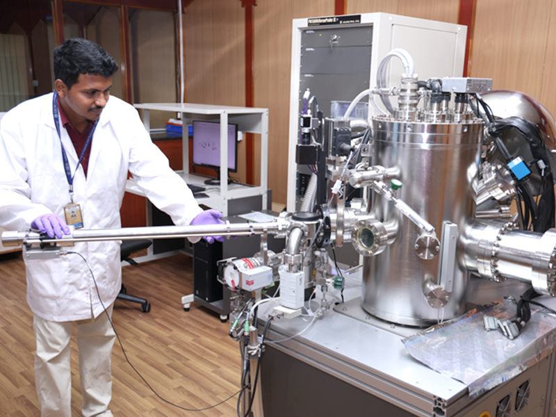
Pulse laser Deposition (PLD) is a physical vapor deposition technique used to deposit thin films of materials onto a substrate. In PLD a high energy laser beam is used to ablate a target material producing a plume of vaporized atoms or ions that are then deposited onto a substrate to form a thin film
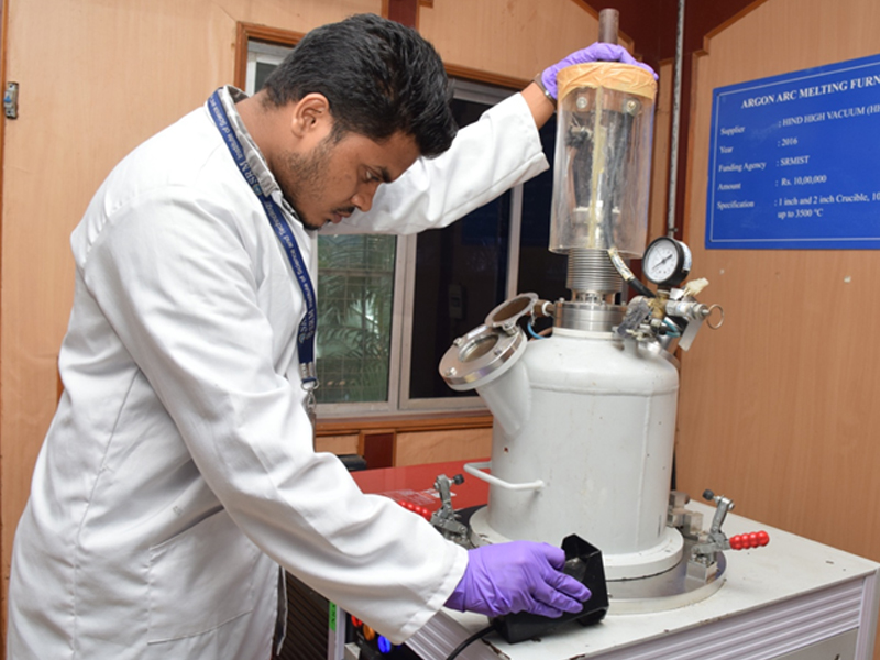
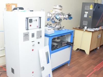
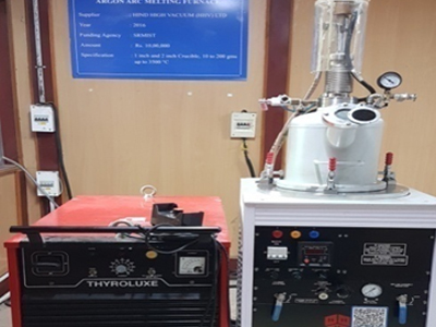
Make: Hind High Vacuum Ltd.
Operation:
An argon arc melting furnace also known as an argon arc furnace or electric arc furnace, is a specialized equipment used for melting and refining metals and alloys under controlled atmospheric conditions. The primary feature of this type of furnace is the use of an electric arc generated between a consumable electrode and the material being melted.
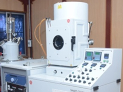
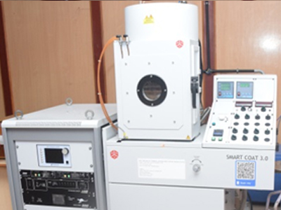
Make: Hind High Vacuum Ltd.
Model: Smart Coat 3.0
Mode: DC & RF
RF/DC sputtering is a physical vapor deposition (PVD) technique used to deposit thin films of materials onto a substrate. The process involves the removal of atoms or molecules from a target material (sputtering target) by bombarding it with high-energy ions, and then these atoms are deposited onto the substrate, create in a thin film. Uses of DC/RF sputtering: Optical electronics, solar cells, sensor devices, magnetic devices and biomedical research.
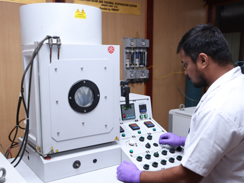
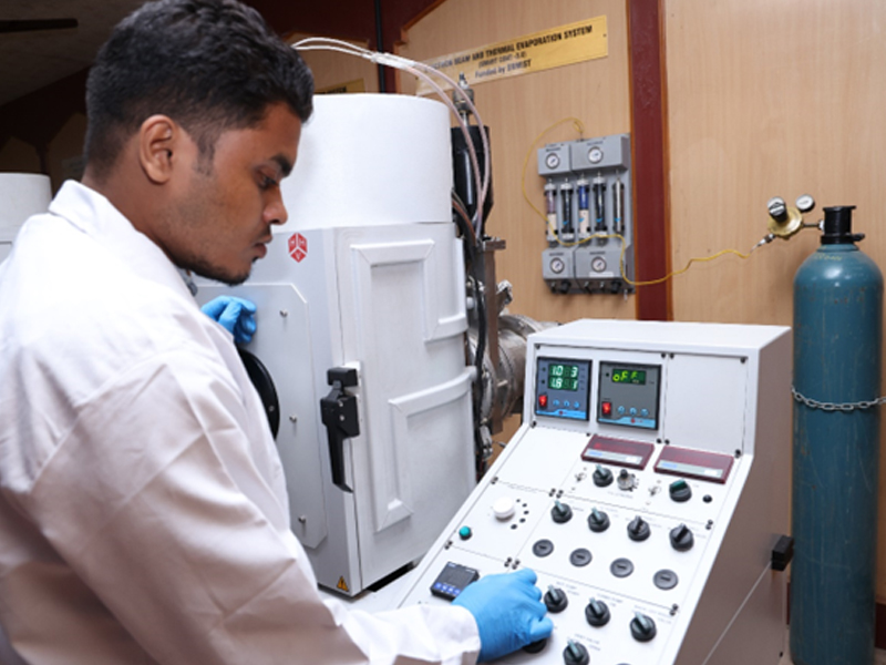
Make: Hind High Vacuum Ltd.
Model: Smart Coat 3.0
Mode: E Beam & Thermal
E-Beam / Thermal Evaporation are used in thin-film deposition process to create thin layers of materials on substrates.
Key features and advantages
High deposition rate: E-beam evaporation can achieve relatively high deposition rates, making it suitable for large-scale production
High-purity films: the vacuum environment prevents contamination,
Good control: Precise control over the deposition rate and thickness of the film is possible
High melting point materials: E-beam evaporation can be used for materials with high melting points that may be challenging for other techniques like thermal evaporation.
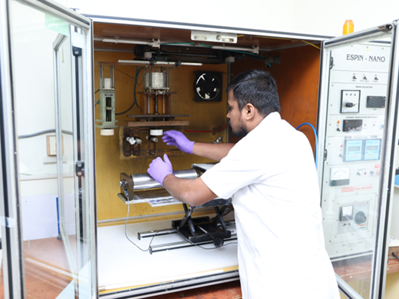
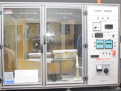
Model: ESPIN NANO
Features
High voltage power supply: 30 kV
Current: 1 mA
Programmable syringe dispersion
Electrospinning is a fibre production method that uses electric force to draw charged threads of polymer solutions or polymer melts up to fibre diameters in the order of some hundred nanometres.
A high vacuum of 1 x 10 -3 m.bar can be maintained within the furnace chamber