


VLSI Simulation Lab
The lab also has a very rich wealth of state-of-art systems and tools for design and testing.
VLSI Simulation Lab
VLSI is an assembly of millions of transistors on a single chip that works flawlessly to realize miracles such as varied multimedia, mobile communication, etc. The VLSI simulation laboratory is established with the aim of conducting research in various aspects of the ever-growing field of Very Large Scale Integration (VLSI) and establishing links between industrial companies. This lab provides basic and advanced facilities for UG and PG coursework-related experiments, B.Tech. and M.Tech. project works, and research facilities in the area of digital & Analog circuit design and various aspects of advanced VLSI design.
Specifications
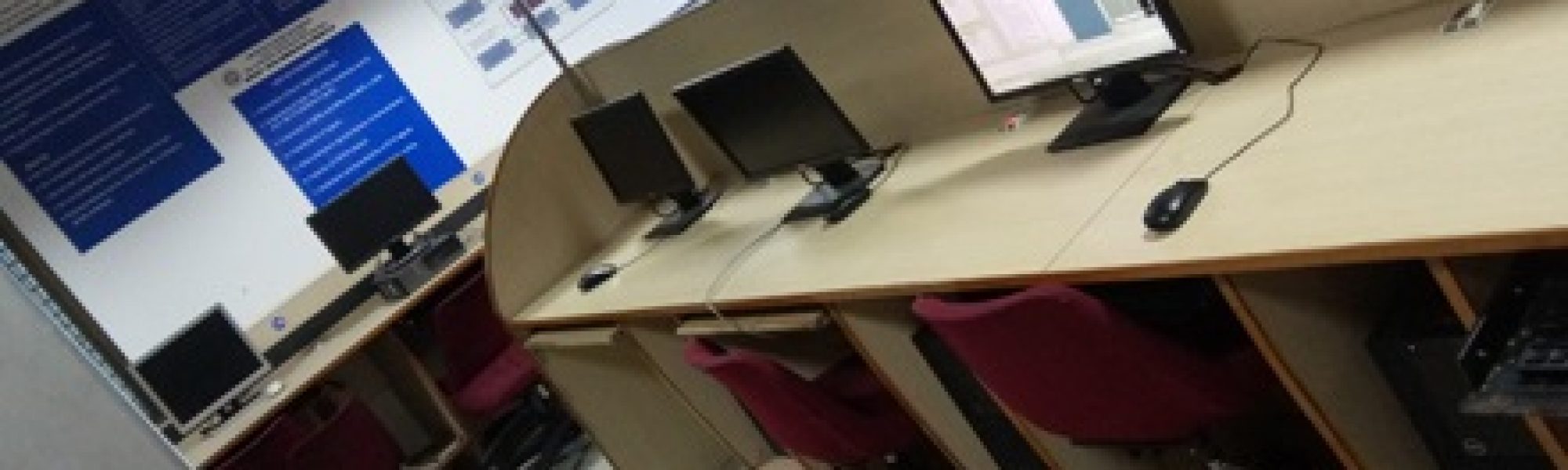
Current Equipments
HP Pro Tower 400 G9 PCI, 12th Gen Intel Core i7 Processor, 512 GB, 1 TB Hard disk, 64 bit operating system, 2.10 GHZ, 16 GB RAM, Micro phone & Headphone Front, LCD color Monitor size 19.5”inch, HP USB Standard keyboard, USB 2 button laser Mouse optical, USB 2 front – 4 ports Rear – 6.
Lenovo Think centre Neo 50 Tower Gen 3 Desktop ,12th Gen Intelcore i7, 16GB RAM,1 TBB HDD, 18” Monitor , Optical Mouse
DELL INTEL (R)Core ™ ,i3-9100@3.60Ghz, 1 TB HDD & 8 GB RAM, DELL Key Board, 18.5” WHD LED Monitor, Optical Mouse, DELL INTEL (R)Core ™ ,i5-4570@3.20Ghz, 500 GB HDD & 4 GB RAM, DELL Key Board, 17” Monitor, Optical Mouse
No data was found
Workstations And Test Equipment
- HP Pro Tower 400 G9 PCI, 12th Gen Intel Core i7 Processor, 512 GB, 1 TB Hard disk, 64 bit operating system, 2.10 GHZ, 16 GB RAM, Micro phone & Headphone Front, LCD color Monitor size 19.5”inch, HP USB Standard keyboard, USB 2 button laser Mouse optical, USB 2 front – 4 ports Rear – 6.
- Lenovo Think centre Neo 50 Tower Gen 3 Desktop ,12th Gen Intelcore i7, 16GB RAM,1 TBB HDD, 18” Monitor , Optical Mouse
- DELL INTEL (R)Core ™ ,i3-9100@3.60Ghz, 1 TB HDD & 8 GB RAM, DELL Key Board, 18.5” WHD LED Monitor, Optical Mouse, DELL INTEL (R)Core ™ ,i5-4570@3.20Ghz, 500 GB HDD & 4 GB RAM, DELL Key Board, 17” Monitor, Optical Mouse
No data was found
Lab Investment: Rs. 32, 03, 998.00/-
- WM2002P Digital Communication Techniques Lab
- EM2002P Microprocessor and Microcontroller Lab
- 20ECC531J Digital Systems Design Using HDL
- 15EC302J VLSI Design Lab
- WM2007 Wireless MIMO Communication Lab
- EM2008 VLSI Design Methodologies and Programming in HDL
- VL2004 CMOS Analog VLSI
- 18ECC206J VLSI Design
- 18ECE206J Advanced Digital System Design
- 18ECE307J Applied Machine Learning
- 18ECC411J FPGA based Embedded systems Design
No data was found
Software
- Mentor Graphics HEP Category 2 Design Software – Design Verification Bundle – Questasim, PrecisionTM Synthesis, Leonardo SpectrumTM, RGQ Tracer, HDL Designer – 50 users License.The Chips to Startup (C2S) Programme is an Indian government initiative aimed at boosting the semiconductor ecosystem in the country. It is part of India’s larger semiconductor mission, introduced under the Ministry of Electronics and Information Technology (MeitY), to promote indigenous chip design and support startups in semiconductor technology. As per the scheme EDA tools will be provided by the ChipIN Centre and will be utilized for teaching, instruction & research purposes by all faculty members, students & researchers at B.Tech, M.Tech, PhD levels and professionals/engineers at the organization.Eligibility criteria for the C2S Programme: The organizations seeking EDA tools from the ChipIN Centre are required to meet the following eligibility criteria:
(i) The organizations should have existing Programs for B.E./ B.Tech or M.E./ M.Tech in Electronics & Communication/ Electrical Engineering/ Microelectronics/ VLSI/ Integrated Circuit/ Embedded System/ Electronic System Design or equivalent.
(ii) The organizations should have the availability of requisite infrastructure & capital equipment for VLSI design lab; as well as permanent faculty members / professionals in VLSI design domain.
The department of ECE, SRMIST has met all the eligibility criteria of the programme and has granted access to following EDA tools from chipIN center.
- Synopsys University bundle-50 License
- Cadence EDA Tools-50 License
Objectives of ECE department under C2S programme: The following are the objectives of the department of the ECE under the programme:
- Focus on VLSI Capacity Building: Train professionals and students in Very Large Scale Integration (VLSI) and semiconductor design.
- Foster Innovation: Encourage startups and the department to innovate in chip design and related technologies such as System-on-Chip (SoC), Integrated Circuits (ICs), Field-Programmable Gate Arrays (FPGAs), and Application-Specific Integrated Circuits (ASICs). Provide access to state-of-the-art EDA tools, prototyping, and testing facilities.
- Self-Reliance: Reduce dependency on imported semiconductor technologies by building domestic expertise.
- Industry-Academia Collaboration: Foster close cooperation between startups, academic institution, and industry partners to address market needs. Drive research and development in emerging semiconductor technologies.
No data was found
No data was found
No data was found
Description
While retaining the salient features of the VLSI Design, this program includes new lecture and laboratory-based courses specially designed to cater to the needs of the industry both in the core program and through electives. We are also offering short-term courses designed to cater to the needs of industries from time to time.
Contact Persons
Mrs. A. Padmavathy
Lab Assistant
padmavaa@srmist.edu.in
Dr. E. Chitra
Assistant Professor
chitrae@srmist.edu.in
No data was found

The VLSI Simulation Laboratory is located in room no. TP1117 Open Door Access: 8:00 am -5:20 pm Scheduled classes take priority.