


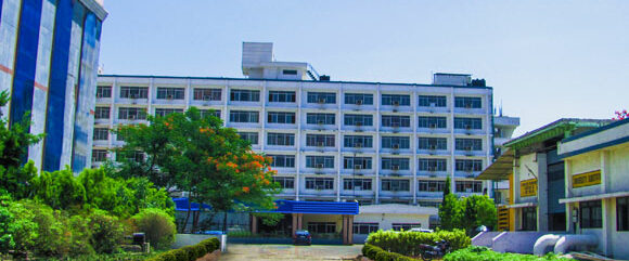


This center is developed to provide holistic experience to the stakeholders on electronics circuit design and manufacturing. Center comprises of specialized laboratory facilitates the design/fabrication/testing facility to crater the need of student project/product development, research works and industrial requirement. This infrastructure can be used to conduct skill development training programs for students, teaching and industry professional in the respective areas in the Electronics design / fabrication / antenna characterization, which helps the stakeholder an industry ready engineer.
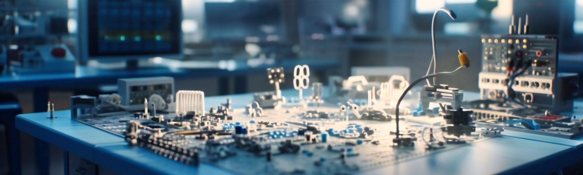
This Lab is equipped with a wide range of Equipment’s, devices, which helps the students to practice electronics circuit design, assembly and testing and also provides a deep insight into the world of electronics practice. It is the skeleton of applied electronics and electronics Engineers. This lab is intended to practice and familiarize to identify the electronic components and to use basic electronic instruments.
This lab is intended to practice and familiarize to identify the FR board selection based on requirement. Thermal circuit transfer method, screen printing method and Directed printing method using Proto typing machine this method different of printing process. PCB fabrication involved various process. Hand on training will be provided to enable the student to impart knowledge in PCB fabrication of the electronic circuits.
Consultancy Service, Research and Development (R&D) by Academic research & Research Institute, Industry. startups, skill development training, internship program.
Date: 02-12-2020
Event: Skill Development Program (PCB Fabrication)


cscesd.ece.ktr@srmist.edu.in
Professor
eswaranp@srmist.edu.in
Project Engineer
dillybak@srmist.edu.in