


Computing Lab (PCB Design)
- Home
- Faculty of Engineering & Technology
- Department of Electronics & Communication
- Computing Lab (PCB Design)
Computing Lab (PCB Design)
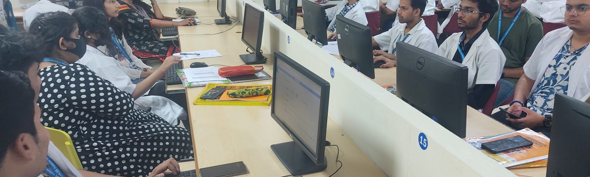
This center is developed to provide holistic experience to the stakeholders on electronics circuit design and manufacturing. Center comprises of specialized laboratory facilitates the design facility to crater the need of student project/product development, research works and industrial requirement. This infrastructure can be used to conduct skill development training programs for students, teaching and industry professional in the respective areas, which helps the stakeholder an industry ready engineer.
Specifications
Current Equipment
The lab is equipped with the following workstations and test equipment
• This lab is facilitated with 22 computers which includes PCB Design computing facility with INTEL (R)Core ™, i5-4570@3.20Ghz, 500 GB HDD & 4 GB RAM configuration system for 20 user licensed TINA software
• PCB Design computing facility with INTEL (R)Core ™, i7-12700 2.10@2.10Ghz, 1 TB HDD; 16 GB RAM configuration system for 1 user licensed Altium software (Commercial)
No data was found
Lab investment: Rs. 1,995,691/-
No data was found
Utilization
This lab is utilized for conducting the following course(s):
- EC1002 – Electronic Engineering Practice Lab
- EC0422 – Project work
- 18ECE231J – IOT system Design
- 18ECO106J – PCB Design and Manufacturing
- 21ECC101J- Electronic System and PCB Design Lab
No data was found
No data was found
No data was found
No data was found
Description
This lab is intended to practice and familiarize with EDA tools for circuit design, simulation and analysis. Student will be exposed to fundamentals of PCB design and various fabrication processes involved. Hand on training will be provided to enable the student to impart knowledge in PCB design of the electronic circuits.
Contact Persons
Mrs T. Aarthy
Assistant Professor
aarthys@srmist.edu.in
Mr. A. Sethuraman
Senior Technical Assistant
sethuraa@srmist.edu.in
No data was found

The Electronic Engineering Practice Laboratory is located in Basic Engineering Laboratory Building, II nd Floor, and Room no. BEL304, Working Hour: 7.45 am - 5:15 pm (Monday to Friday) 9:00 am - 5:00 pm (Saturday) - Scheduled classes take priority